News and events
.webp)
Apr 07, 2026
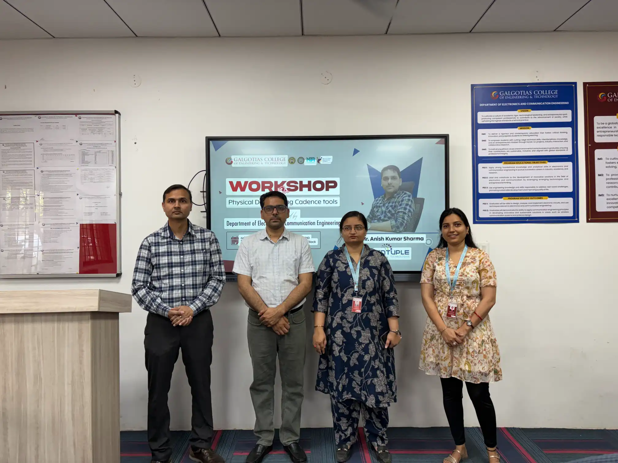
Workshop on Physical Design Using Cadence Tools
Events | Apr 06, 2026
Event Date: Monday, 6th April 2026
Time: 10:00 AM Onwards
Venue: 010, B-Block, GCET Campus
Hands-On Exposure to Industry-Relevant VLSI Design Tools and Semiconductor Physical Design Concepts
Event Brief Description
The Department of Electronics and Communication Engineering, Galgotias College of Engineering and Technology (GCET), organized a Workshop on "Physical Design Using Cadence Tools" on Monday, 6th April 2026, at 010, B-Block, GCET Campus, commencing at 10:00 AM. The workshop aimed to provide students with hands-on exposure to industry-relevant VLSI design tools and enhance their practical understanding of physical design concepts used in semiconductor engineering.
The session was conducted by Mr. Anish Kumar Sharma from Entuple Technologies, who shared valuable insights into Cadence tools and their real-world applications in semiconductor design. The workshop offered students a practical learning environment that bridged the gap between academic knowledge and the skills required in the VLSI and semiconductor industry.
Event Detailed Description
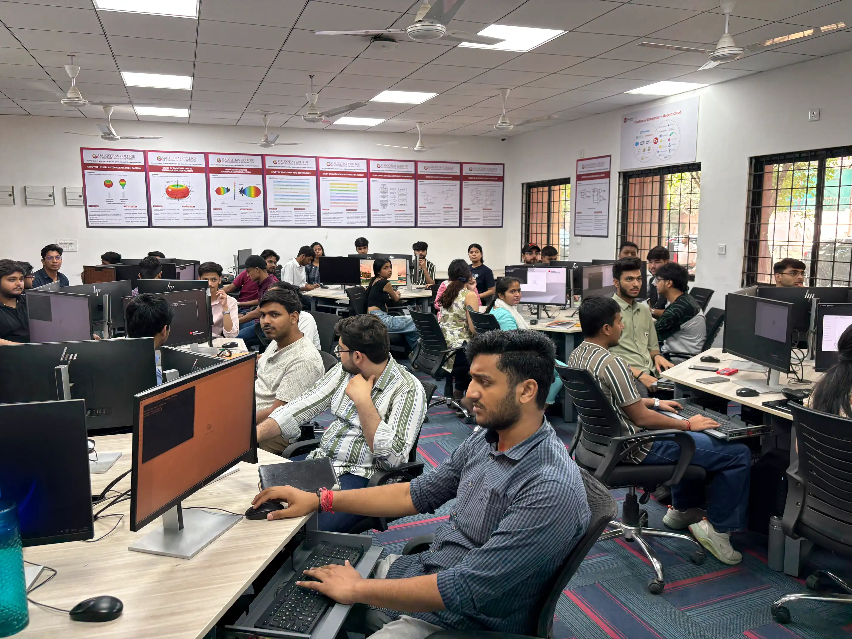
The Workshop on Physical Design Using Cadence Tools was organized by the Department of Electronics and Communication Engineering, GCET, on 6th April 2026. The session began at 10:00 AM at Room 010, B-Block, and was attended by students of the ECE department along with faculty members. The workshop was designed to provide students with practical, hands-on exposure to Cadence tools, which are widely used in the VLSI and semiconductor design industry.
Mr. Anish Kumar Sharma, representing Entuple Technologies, conducted the workshop with an in-depth and structured approach to the subject. He began with an introduction to Physical Design, covering the complete VLSI design flow from RTL to GDSII, including key stages such as floorplanning, placement, clock tree synthesis (CTS), routing, and sign-off. He explained the significance of each stage in ensuring the correctness and manufacturability of semiconductor chips.
A significant portion of the workshop was dedicated to hands-on training on Cadence tools, which are the industry standard for physical design and verification. Students were guided through the practical use of Cadence Innovus for implementation and Cadence Virtuoso for layout design, gaining direct experience with the tools used by engineers at leading semiconductor companies. Mr. Sharma demonstrated real-world design scenarios and walked students through the step-by-step process of creating and verifying a physical design layout.
Mr. Sharma also discussed the current landscape of the semiconductor industry, the growing demand for VLSI design engineers, and the specific skills and tools knowledge that companies look for when hiring freshers and experienced professionals. He emphasized the importance of gaining hands-on experience with EDA tools like Cadence early in one's academic career to stand out in the competitive VLSI job market.
The workshop included an interactive session where students asked questions related to career pathways in VLSI design, internship opportunities, and the role of Entuple Technologies in the semiconductor ecosystem. The event concluded on an encouraging note, with students gaining both technical knowledge and career clarity in the domain of physical design and semiconductor engineering. The Department of Electronics and Communication Engineering expressed its gratitude to Mr. Anish Kumar Sharma and Entuple Technologies for their valuable contribution to the students' learning experience.
Department Name: Department of Electronics and Communication Engineering (ECE), Galgotias College of Engineering and Technology (GCET)
Resource Person: Mr. Anish Kumar Sharma, Entuple Technologies
Event Outcomes
- Hands-On Exposure to Cadence Tools: Students gained practical, hands-on experience with industry-standard Cadence tools including Cadence Innovus and Cadence Virtuoso, equipping them with the tool knowledge required for VLSI physical design roles in the semiconductor industry.
- Understanding of the Physical Design Flow: Students developed a comprehensive understanding of the end-to-end VLSI physical design flow from RTL to GDSII, including floorplanning, placement, clock tree synthesis, routing, and sign-off, enhancing their conceptual and practical knowledge of semiconductor chip design.
- Awareness of Industry Requirements and Career Pathways: Students gained valuable insights into the current semiconductor industry landscape, the demand for VLSI design engineers, and the specific skills and tool proficiencies that top companies expect from candidates, helping them chart a clearer career roadmap.
- Bridging the Gap between Academia and Industry: The workshop effectively connected theoretical VLSI concepts taught in the ECE curriculum with real-world semiconductor design practices, enabling students to understand how academic knowledge translates into professional engineering work.
- Motivation to Pursue VLSI as a Career: The interactive session and real-world examples shared by Mr. Anish Kumar Sharma inspired students to explore internships, projects, and certifications in VLSI and physical design, and to consider semiconductor engineering as a promising career option.